News & information from UB, New York's flagship university
Electronic Packaging Lab at UB Developing Ways to Make Electronic Devices Smaller, Faster and More Reliable
Intel using UB research in its next-generation Pentium processor
Release Date: September 3, 2003 This content is archived.


BUFFALO, N.Y. -- Some of the world's most advanced research in micro- and nanoelectronic-packaging reliability is taking place in the Electronic Packaging Laboratory in the University at Buffalo School of Engineering and Applied Sciences.
UB engineers are addressing critical problems confronting the electronics industry as it attempts to make electronic packages -- the bundles of circuits, connections and bonds within electronic devices -- much smaller and more reliable. Their research is helping to reduce the size and increase the speed and life span of electronic devices, and is opening the door for the creation of new devices.
Currently, Intel is using the UB lab's research to develop the next-generation packaging for its Pentium processor. The UB researchers also are working to break industry bottlenecks impeding development of revolutionary systems and products, such as lead-free packages, nanoscale computers and even implantable bio-electronic devices -- including cell phones and electronic eyes that work within the body and communicate directly with the brain's auditory and optical nerves.
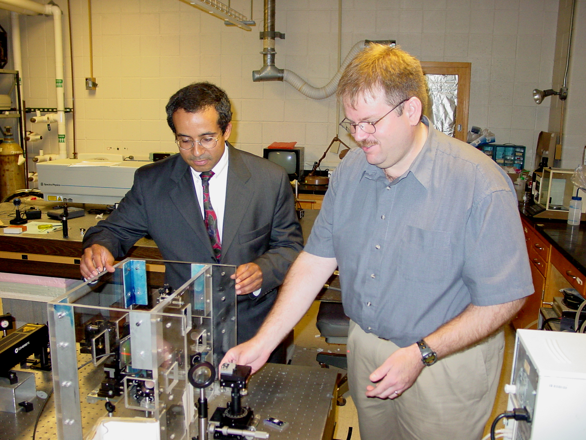
"No one else in the world is doing what we're doing," says Cemal Basaran, director of UB Electronics Packaging Laboratory and an associate professor of civil, structural and environmental engineering.
Basaran and lab co-director Alexander Cartwright, UB associate professor of electrical engineering, are revolutionizing the design of solder joints that connect circuits to electrical boards within a device. High electrical-current density and heat produced by the circuits over time breaks down solder joints, leading to system failure. The damaging effects of high current density and heat also limit attempts to make electronic packages smaller and faster, Cartwright notes.
"Solder joints are the biggest bottleneck and source of failure in microelectronics," Cartwright says. "The chips themselves don't fail; it's where the chips interact on the board that the failure occurs.
"If we can give interconnections and contacts the same speed and reliability as the chips, computers would be much faster and rarely would fail."
According to Basaran, the relationship between high electrical-current density and mechanical degradation has never been studied for solder joints at the engineering-mechanics level. The UB researchers are the first to measure the strain field in a microelectronic solder joint due to high electrical-current density. They also are the first to attempt to model and simulate the damage done to solder joints.
"Developing very small, yet super fast, electronics requires understanding the failure mechanisms at the high current density levels we will see in next generation electronics," Basaran says.
Using a process called moiré interferometry -- which uses laser beams to measure the displacement field of solder material -- the UB researchers are able to measure strain within solder joints as they are exposed to simulated service conditions.
They have developed a novel methodology for measuring the stress and strain imposed on electronics packaging under near-exact operating conditions and with displacement resolution down to 27 nanometers.
"We want to measure the amount of damage done to the package during thermal and vibration loading, when there is high current," explains Basaran. "It's very difficult to do, but we have developed a technique to do it at nanoscale and we're doing it in real-time."
As the researchers "look down" on the joints at the nanoscale, they notice interesting transformations. Electromigration of the solder begins to occur, with the solder material shifting slowly downward toward the board and creating voids within the solder. Too many voids force the electrical current to find new ways to travel within the solder. Or, electrons become trapped between voids within the solder.
"Anytime you have defects, it accelerates a breakdown of the package and soon you have failure," Cartwright says.
Using this and other research results from the UB lab, Basaran and his doctoral students have developed computer models to simulate and predict package-fatigue life and reliability under service conditions.
Their methods and results are generating interest throughout the electronics industry, and have attracted significant funding from many corporations and government entities, including Intel, Micron, the U.S. Navy, the U.S. Department of Defense, the National Science Foundation and New York State.
"With the computer models, we can design a complete system without having to build more than one prototype," Basaran says. "These models can produce a huge savings for companies in terms of development costs, product testing and time to market. It cuts down time-to-market from three years to one to six months."
From this research, Cartwright and Basaran have developed high-sensitivity inspection technologies and computer simulation models -- implemented and utilized by Intel and other companies -- for designing the next generation microelectronics packaging.
The UB Packaging Lab, Basaran says, will continue to work with Intel and others to improve the reliability and to reduce the size of microelectronics, but the lab also has begun to focus on new areas of research.
With the European Union and Japan expected to ban lead components next year, the UB lab is among those racing to develop an understanding of the mechanical properties of lead-free solder, and is experimenting with tin-silver and copper solder composites.
And, according to Basaran, the UB lab is working on nanoscale packages that may lead to the creation of supercomputers as small as a wristwatch.
"Nanoelectronics is the future," he says. "Once we have reliable packages at the nanoscale, we can do many, many things."
For more information about the UB Electronic Packaging Lab, go to http://www.packaging.buffalo.edu.
Media Contact Information
John Della Contrada
Vice President for University Communications
521 Capen Hall
Buffalo, NY 14260
Tel: 716-645-4094 (mobile: 716-361-3006)
dellacon@buffalo.edu
www.linkedin.com/in/john-dellacontrada

