Cleanroom Fundamentals and Semiconductor Technologies
Self-Paced Online Course
Cleanroom Fundamentals and Semiconductor Technologies is a comprehensive nine-hour online course from the University at Buffalo that builds a strong foundation in modern semiconductor manufacturing and cleanroom operations. Designed for students, engineers, technicians, and professionals entering or supporting the semiconductor industry, the course explains how silicon-based devices are designed, fabricated, and manufactured in advanced cleanroom environments.
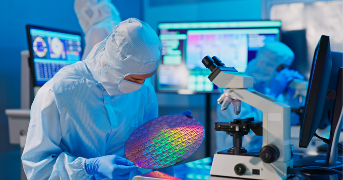
Learners receive a structured introduction to the physics and processes behind today’s microelectronics, including transistor fundamentals, cleanroom classifications and design, semiconductor materials, and vacuum science. Key wafer-processing techniques are covered, such as thin-film deposition (PVD and CVD), doping, thermal oxidation, wet and dry etching, and photolithography — the critical patterning step in device fabrication.
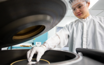
A standout feature of the course is its virtual, hands-on lab experience, where participants apply concepts in a simulated cleanroom. Guided exercises in photolithography and etching provide practical exposure to wafer-processing workflows, helping bridge theory and real-world practice.
By the end of the course, learners gain a well-rounded understanding of cleanroom operations and semiconductor fabrication, preparing them to engage confidently with industry-standard technologies in academic, research, or industrial settings. A UB certificate is earned upon completion.
Course Layout
Topics include:
| Transistors | Understand How Transistors Behave as a Switch |
| Cleanrooms | Learn the Fundamental Principles of Cleanroom Design and Operation, with a Focus on Filtration, Airflow Patterns, and Pressurization Control |
| Semiconductor Materials | Gain Insights on the Production Processes of Ultrapure Silicon and the Additional Materials Used in Transistor Fabrication |
| Vacuum Science Overview | Learn the Purpose and Functioning of Vacuum Systems in Semiconductor Fabrication Processes |
| Physical Vapor Deposition (PVD) | Explore the Basic Principles Behind Evaporation and Sputter PVD processes, as well as the Function of Vacuum Process Control Systems |
Topics include:
| Chemical Vapor Deposition (CVD) | Familiarize Yourself with the Basics of CVD Processes, Including the Chemistry Involved and the Essential Equipment Used |
| Doping | Learn What Doping Is and How It Is Accomplished |
| Oxidation | Learn the Core Concepts of Thermal Oxidation of Silicon and Contact Sintering |
| Wet Processing | Grasp the Key Principles of Liquid-based Chemical Cleaning and Etching Techniques |
| Dry Etching | Discover how Plasmas Work and Their Role in Etching Materials |
| Photolithography | Understand the Processes and Techniques for Creating Patterns on Semiconductor Materials |
Techniques include:
| Photolithography Bay (Yellow Light) |
|
| Etch Bay (White Light) |
|
About the Instructor:
Jeff Salzmann, Assistant Professor of Research

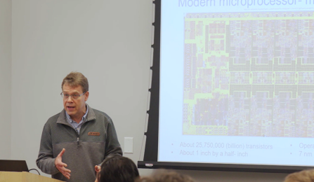
Jeff brings over 30 years of semiconductor and facility experience to the university, in roles such as process engineering, technology development, device development, and fundamental research. He holds an AS in Engineering Science from SUNY Erie, a BS in Microelectronic Engineering from Rochester Institute of Technology, and an MS in Materials Science and Engineering from Rochester Institute of Technology. He has worked for such companies as IBM, Digital Equipment Corporation, Corning, Greatbatch, Integer, and the National Security Agency. His hobbies include drumming, photography, and cooking.