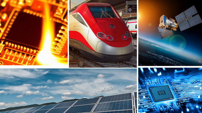
Researchers within the Center advance modern microelectronics by engaging in research across a variety of domains:
The development of functional (low-dimensional) electronic materials, including atomically thin 2D materials, magnetic and widegap semiconductors, perovskite-based solar absorbers and non-volatile and phase-change materials
The exploration of beyond-complementary metal-oxide-semiconductor (CMOS) transistor concepts, including spintronic devices, tunneling transistors, plasmonic devices for terahertz communications, radiation-hard devices for space-based applications, hot-carrier solar cells and quantum devices for advanced metrology.
CMOS + X circuit concepts that enable functionality such as low-power operation, circuit non-volatility, and substantial area savings compared to CMOS
New York state's ambitious goals to achieve net-zero emissions by 2050 provide a common theme connecting many of these efforts.
Researchers are developing advanced wide bandgap and ultra-wide bandgap semiconductor devices and circuits for high-power and high-frequency applications. This work focuses on overcoming performance limitations of conventional semiconductor technologies and enabling more efficient power electronics, communication systems, and next-generation energy solutions.
The research theme develops innovative devices and circuit architectures designed to reduce power consumption while maintaining or improving system performance. These efforts support sustainable computing and electronics technologies that are increasingly critical for data centers, communication networks, and intelligent systems.
Researchers are advancing semiconductor photovoltaic devices and circuits to deliver reliable and efficient energy generation for demanding environments, including space applications. This work addresses challenges in energy harvesting, power conversion and system integration.
This research theme explores the fundamental materials science and physical phenomena that drive semiconductor performance. By understanding and engineering material properties at the microscopic level, researchers aim to enable future generations of semiconductor devices with enhanced speed, efficiency, reliability, and functionality.