
 "They were trying to glue a semiconductor to another piece of
semiconductor, but it didn't glue very well and it just came off," recalled
Hong Luo, assistant professor of physics, who led the group with Athous
Petrou, professor of physics. "They thought it was ruined."
"They were trying to glue a semiconductor to another piece of
semiconductor, but it didn't glue very well and it just came off," recalled
Hong Luo, assistant professor of physics, who led the group with Athous
Petrou, professor of physics. "They thought it was ruined."
Despite that feeling, the next day the students exercised their scientific curiosity and tested the "ruined" semiconductor for optical properties, only to find they were still intact.
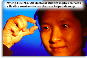
The UB team had, they discovered, created the world's first flexible semiconductor.
The first single-crystal, semiconducting nanomaterials that bend, but don't break were described recently in Applied Physics Letters.
They can be peeled right off their supports almost as though one were peeling an address label from a sheet of labels and some of them were made using ordinary weatherstripping silicone.
Semiconductors lie at the heart of micro-electronic devices. "When we think of semiconductors, we think of a crystal, something that is very hard and very fragile," said Luo. "But these semiconductors can bend like rubber."
Because they retain both their structural integrity and optical prop erties, the semiconductors are seen as particularly significant for future advances in optical computing, where information will be carried by light instead of by electrons.
"These semiconductors could help expedite the transition from electronics to optical computers by allowing us to exploit optics in semiconductors much more efficiently than has been possible," said Luo.
The new semiconductors are ideal for optical computing because they will allow for optical waveguides-the optical equivalent of wires-and semiconductors to be contained inside the same component.
Their flexibility also makes it possible to transmit optical signals in three-dimensional optical circuits, making their applications far more efficient and allowing for far more versatile design than now is possible with two-dimensional transmission of light.
Other applications lie in optical waveguides for telecommunications and in high-efficiency solar cells for the military, which should be lightweight but sturdy and flexible enough to withstand rocket blastoff and battlefield conditions.
"We have developed a general technology to be used with all semiconductors," Luo explained.
He said the new semiconductors are flexible because they are deposited on substrates in such thin layers by molecular-beam epitaxy (MBE), a technique that involves the deposition of thin films on substrates in an ultra-high-vacuum chamber.
"Theoretically, if you could make it thin enough, even a diamond could be flexible," he said. "But such thin materials are, of course, extremely fragile. They need to be supported by something, which makes it a physicist's problem. We have figured out a way to give mechanical support to this type of semiconductor structure."
"The flexible semiconductors we developed are man-made structures that are fabricated using conventional semiconducting elements," he said. "Such materials possess superior optical properties and can be combined with polymeric materials because both are flexible."
So far, the UB researchers have fabricated semiconductors that are about one centimeter in diameter, but Luo said that in facilities used to make industrial products, samples of up to five inches in diameter and even larger could be fabricated.
Co-authors on the paper, which appeared in the September issue of Applied Physics Letters, are Jens J. Haetty, Myung-Hee Na and Huicheng Chang, all doctoral candidates in physics at UB.